
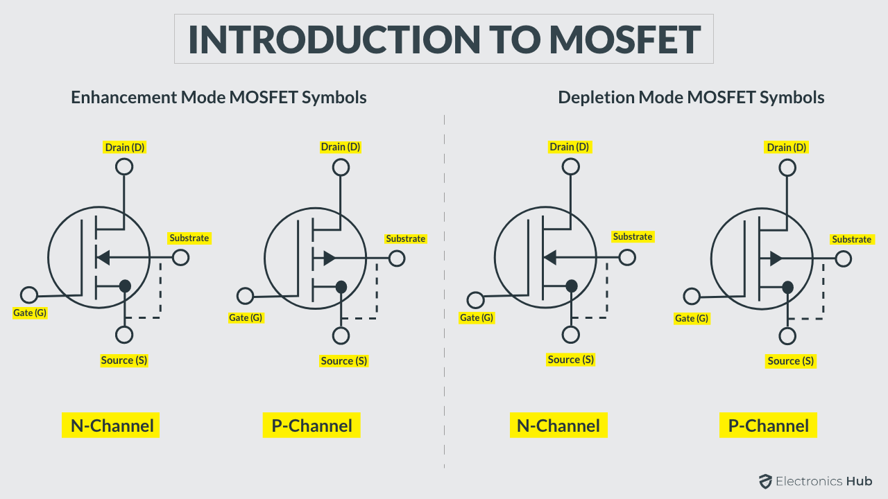
How electrons move through an N-type MOSFET channel
I was sitting on my bench last Tuesday, staring at a power supply that kept tripping. The MOSFET in my hand was borrowed from a scrap board, but it was working fine. The issue wasn’t the device—it was me not respecting how electrons actually behave inside that channel. Ten years of designing switching regulators, motor drivers, and RF amplifiers, and I still catch myself glossing over the basics. Let’s fix that today.
If you want to understand how an N-type MOSFET turns on and conducts, you need to stop thinking about it as a magic switch. It’s a carefully engineered water slide for electrons—with gates, voltage gradients, and a material that either helps or hinders the ride. The physics is beautiful once you stop running from it.
Look— the key is the formation of the inversion layer. Without that, you have nothing. No channel. No conduction. Just two islands of silicon with a barrier between them. So let’s walk through it step by step, the way I teach it to my junior engineers.
The Physics Behind the Movement: Understanding the Inversion Layer
The N-type MOSFET starts with a p-type substrate. That might sound backwards for an N-type device, but that’s exactly the point. The source and drain are heavily doped n+ regions, but they’re separated by the p‑type body. Between source and drain, there’s no direct path for electrons to travel. It’s an open circuit.
Now you apply a positive voltage to the gate. What happens next is almost poetic. The electric field from the gate pushes the holes in the p‑type substrate away from the silicon surface. The holes get repelled downward into the bulk. This leaves behind a thin layer of immobile, negatively charged acceptor ions at the silicon‑oxide interface. That layer is called the depletion region.
But we need more than just a depletion region—we need a conductive channel. Keep increasing the gate voltage above the threshold voltage (Vth) . The electric field becomes strong enough to attract minority carriers—in this case, electrons—from the p‑type body. These electrons gather right at the surface. It’s a thin layer of them, so thin you could measure it in angstroms. This thin layer is the inversion layer, and it connects the n+ source to the n+ drain.
Seriously, this is the single most counterintuitive part of MOSFET operation. We’re using a p‑type material and, through brute force of voltage, turning the surface of that material into an n‑type material. The electrons that form the channel come from the substrate itself, diffusing or drifting into place.
Gate Voltage and the Creation of a Channel
If you want electrons to move efficiently, you need the channel to exist first. The gate voltage is the boss here. You raise Vgs above Vth, and the inversion layer forms. You drop Vgs below Vth, and the channel vanishes. It’s that binary. That’s why we call it a threshold.
Think of the gate as the conductor of an orchestra. The electrons are the musicians. At low voltages, the orchestra is silent. At the threshold, the musicians start to pick up their instruments. But they aren’t playing yet—they’re just sitting there, ready. The actual movement of electrons from source to drain requires a second voltage: Vds, the drain-to-source voltage.
Once the inversion layer is formed, the channel behaves like a thin sheet of conductive material. The charge density in the channel is set by the gate voltage. Higher Vgs means more electrons in the channel. More electrons means lower resistance. It’s a voltage‑controlled resistor at low drain voltages.
Why Electrons Move (and Not Holes)
This is where people get confused. In an N-type MOSFET, the current is carried by electrons. The holes are essentially spectators. The holes get pushed out of the way during the inversion process, and they contribute nothing to the drain current. That’s by design.
The mobility of electrons in silicon is roughly three times higher than the mobility of holes. That means you get more current for the same voltage. That’s why N-type MOSFETs switch faster and have lower on‑resistance than their P‑type counterparts. Electrons are lighter, faster, and more responsive. It’s physics working in your favor.
So when you see a data sheet for an N‑channel MOSFET with remarkably low Rds(on), thank the electrons. They are doing the heavy lifting, moving from source to drain through that fragile but essential inversion layer.
Ohmic vs. Saturation: How Voltage Alters Electron Flow
Now that the channel is there, what happens when you actually apply a voltage between drain and source? The electrons start to feel a lateral electric field. They are pulled from the source (low potential) toward the drain (high potential). At low Vds, the channel behaves like a resistor. The electron current increases linearly with drain voltage. This is the linear region, also called the ohmic region.
But here’s the secret: the channel isn’t uniform. As electrons move toward the drain, they experience a voltage drop along the way. The potential difference between the gate and the channel decreases as you approach the drain. The inversion layer gets thinner near the drain end. It pinches down.
Eventually, you reach a point where increasing Vds no longer increases the drain current. The channel has pinched off. The electrons are now moving through a very short, high‑field region near the drain. This is the saturation region. The electron velocity in that region is saturated—it reaches a maximum value thanks to scattering effects in the silicon lattice.
- In the linear region, the electrons move relatively slowly, and the channel acts as a resistor. - In the saturation region, the electrons are moving at their maximum drift velocity, and the current is essentially constant. - The transition happens when Vds reaches roughly (Vgs - Vth). That’s the overdrive voltage.
It’s a big deal because this behavior dictates everything about amplifier design, switch timing, and power dissipation. Ignore the saturation region, and your design will fail.
The Linear Region: A Voltage-Controlled Resistor
At very low drain voltages, the electrons in the channel don’t have to fight much. The inversion layer is thick and uniform from source to drain. The current follows Ohm’s law directly: Id = C (Vgs - Vth) Vds, where C is a constant related to the geometry and oxide capacitance.
This is why engineers use MOSFETs as analog switches and pass gates. If you keep Vds small (typically under 100 mV), the device behaves like a resistor whose value you set with the gate voltage. The electron density is high, and the drift velocity is proportional to the electric field.
For a practical example, think of a 2N7002 used as a low‑side switch. With Vgs = 10V and Vds = 50 mV, the electrons experience a gentle, nearly uniform field. The Rds(on) might be a few ohms. The electron current is just a straightforward linear function of voltage.
Honestly, the math is beautiful here. It’s the simplest operating mode, and it’s the most predictable. No pinch‑off, no velocity saturation, no complex behavior. Just resistance.
Saturation: When the Current Just Won’t Listen
As Vds climbs above the overdrive voltage, things get weird. The channel pinches off near the drain. The electrons are now flowing through a tiny depletion region at the drain end. The current doesn’t increase because the electron drift velocity is maxed out.
This is velocity saturation. In short‑channel devices (below 0.5 micron), this happens very quickly. The electrons hit their maximum velocity at relatively low fields. The current becomes essentially independent of Vds. The MOSFET now acts like a current source—a constant current between drain and source, controlled solely by Vgs.
A quick list of what the electrons encounter in saturation:
- Velocity saturation limits the maximum current - Channel length modulation means the pinch‑off point moves slightly as Vds increases, causing a small increase in current - Gate field modulation can still affect the carrier concentration near the source
So if you’re designing an amplifier that needs high gain, you operate in saturation. If you’re designing a power switch for minimal losses, you operate in the linear region. The electrons don’t care—they just respond to the fields you create. It’s your job to set them up for success.
The Role of the Drain and Source Voltages
You cannot talk about electron movement without understanding the asymmetry of the MOSFET. The source is the electron supply. The drain is the electron sink. In an N‑type device, the source is at the lower potential (usually ground), and the drain is at the higher potential.
The electrons flow from source to drain. The conventional current flows from drain to source. Keep that straight, or you will make mistakes.
The source voltage is critical because it sets the body effect. If the source is above the body (substrate) potential, the threshold voltage increases. The inversion layer gets harder to form. Electrons have a tougher time accumulating at the surface. This is why you always want the source and body tied together in your discrete designs.
- The source provides the electrons for the channel. - The drain collects the electrons after they traverse the channel. - The body affects the threshold voltage and, consequently, the electron density.
A practical takeaway: never leave the body floating in an integrated circuit. Floating bodies cause kink effects and latch‑up. Electrons can find unintended paths, and your circuit dies. I learned that the hard way on a 12V boost converter prototype.
Common Questions About How electrons move through an N-type MOSFET channel
#### What actually makes the electrons start moving through the channel?
The electrons start moving when the drain voltage (Vds) creates a lateral electric field along the channel. The gate voltage (above Vth) already has the electrons sitting in the inversion layer. As soon as the drain voltage appears, the electrons feel a force from the high‑potential drain toward the lower‑potential source. They accelerate and start flowing as drift current.
#### Why does the current saturate in a MOSFET?
Saturation occurs because the inversion layer pinches off near the drain. The voltage between the gate and the channel drops below Vth at the drain end. The electrons must then travel through the high‑field depletion region. Their velocity reaches a maximum (velocity saturation), or the channel simply cannot provide any more carriers. The current stops increasing with Vds.
#### What is pinch-off, exactly?
Pinch‑off happens when the drain voltage is high enough that the inversion layer gets so thin near the drain that it disappears. The electrons are no longer in a continuous conductive sheet. Instead, they are injected into a depletion region where the electric field is extremely high. They zip across that gap, but the overall current is limited by how many electrons the source can inject into the channel.
#### How does temperature affect electron movement in the channel?
Higher temperature reduces carrier mobility. The electrons scatter more off phonons (lattice vibrations). This reduces the current for a given voltage. However, higher temperature also increases the threshold voltage slightly, which further reduces current. The net effect is that MOSFETs have a positive temperature coefficient above a certain current level, which actually helps prevent thermal runaway in power devices.
#### Does the current flow through the entire depth of the substrate?
No. The electron current is confined to the inversion layer at the surface of the silicon, directly under the gate oxide. The depth of this channel is typically 5 to 10 nanometers. Below that, the p‑type body has very few free electrons and is essentially an insulator. The channel is a two‑dimensional electron gas, not a bulk conductor. That’s why the MOSFET behaves like a surface‑controlled device.
Instead, electrons exist in specific regions of probability around the nucleus called orbitals, which are. The excitation of core electrons is possible, but requires much. That is, ψ(r1, r2) = −ψ(r2, r1), where the variables r1 and r2 correspond. Electrons can separate from atoms because of the way they surround nuclei. Electrons are considered to be a type of elementary particle because they are not made up of smaller components. The wave function of fermions, including electrons, is antisymmetric, meaning that it changes sign when two electrons are swapped; Usually, the excitation of valence electrons (such as 3s for sodium) involves energies corresponding to photons of visible or ultraviolet light. These free electrons mix with ions to form a plasma. This model has successfully explained the behavior of electrons in atoms and molecules, and it forms the basis of our understanding of chemical bonding and the flow of electrons in materials. Electrons do not orbit the nucleus of an atom in the same way planets orbit the sun.