
What is MOSFET Pinch-Off and How Does It Occur
You've probably seen the curve on a datasheet — that flat region where no matter how much you increase the drain voltage, the current just won't budge. That's MOSFET pinch-off in action. Honestly? Most textbooks make this sound like a magic trick involving invisible scissors. It's not magic. It's a straightforward piece of semiconductor physics, and once you see it clearly, you'll never unsee it.
Here's the core idea: pinch-off doesn't mean cutting off current. It means pinching the conductive channel so hard that the current becomes constant — a fixed, saturated value. This phenomenon defines how a MOSFET behaves as an amplifier or as a current source. Without it, your smartphone, your laptop, your entire digital world would be a hot, uncontrollable mess.
Let's dig into the mechanics, the math, and the real-world meaning of this critical effect. I'll show you exactly where and why it happens, with no fluff.
The Basic Mechanism: What Exactly Is Pinch-Off?
MOSFET pinch-off is a condition that occurs in the channel of a field-effect transistor when the drain-to-source voltage (Vds) becomes high enough to effectively "strangle" the channel near the drain end. The channel doesn't vanish — it narrows to a point where it can't deliver any more current carriers. Current, however, still flows because the remaining carriers get swept across by the electric field. Serious business.
Think of it like a garden hose. You turn the faucet (that's your gate voltage) to set a certain flow rate. Now you pinch the hose near the nozzle (that's your drain voltage). The water doesn't stop — it shoots out faster and at a constant rate because the hose cross-section is reduced. That stretched, thin section is your pinch-off region. The flow rate is determined entirely by the faucet, not by how hard you squeeze. That's the essence of it.
The key distinction is that pinch-off is not the same as cutoff. In cutoff, you've turned the gate voltage off completely (below threshold) and the channel simply doesn't exist — zero current. In pinch-off, the channel is fully formed near the source but gets compressed to near-zero thickness at the drain end. The transistor is still very much "on" and conducting, just in a different mode. It's a big deal.
So when someone says the MOSFET is "pinched off," they mean the drain end of the channel has lost its free-carrier concentration (inversion layer). Let's get into the specific conditions that create this. Look—it all comes down to a voltage gradient along the channel and the fundamental rules of how oxide and silicon interact.
Why the Channel Pinches at the Drain End First
The channel in a MOSFET isn't a uniform pipe. It's a resistive slab under the gate oxide. When you apply a drain voltage, the voltage along the channel drops from the drain voltage at the drain end to zero at the source end. Seriously, it's just Ohm's law in action over a distributed resistor. This voltage drop directly affects the local gate-to-channel voltage (Vgc).
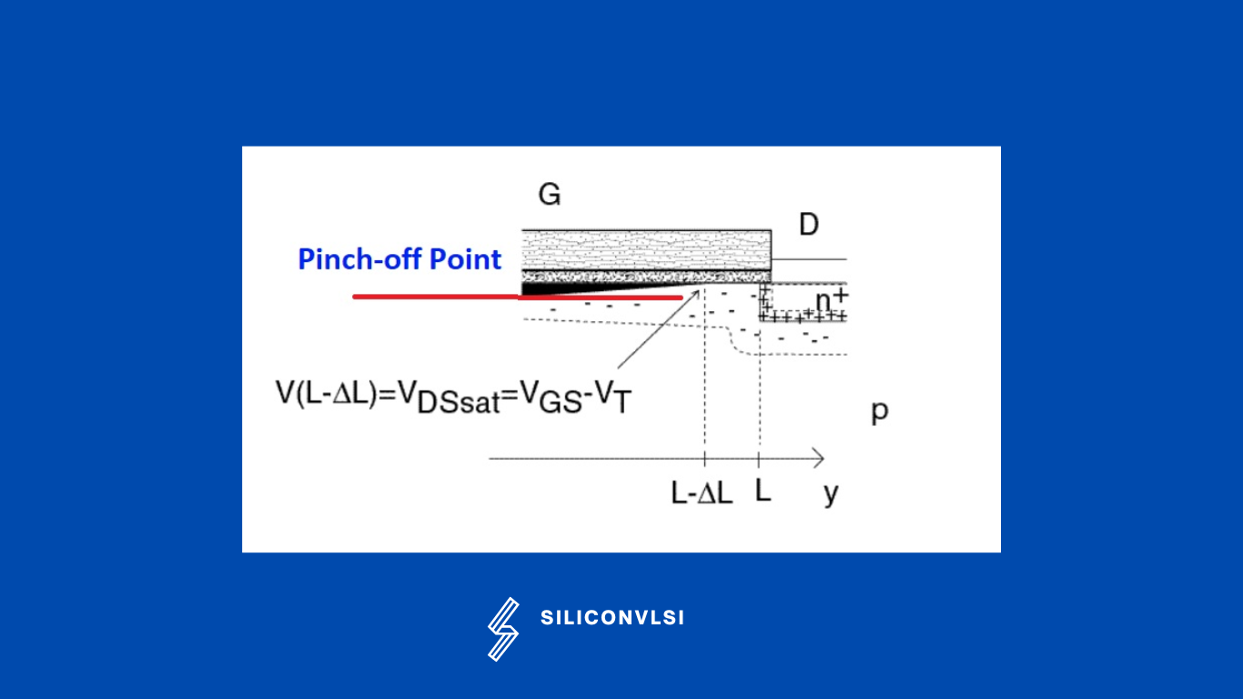
Near the source, Vgc is high: the gate sees the full gate voltage minus zero volts. That strong field maintains a healthy inversion layer with plenty of mobile carriers. But near the drain, Vgc is lower: the gate voltage minus the large drain voltage. If Vds gets high enough, the Vgc near the drain drops below the threshold voltage (Vth). When that happens, the inversion layer can't exist there anymore. The channel literally disappears at that point. It's a fundamental limit.
So the pinch-off point — the location where the channel thickness goes to zero — isn't fixed. It moves closer to the source as you increase Vds. This is the birth of channel length modulation, the effect that makes real-world current sources not perfectly flat. But that's a subtlety for later. The core physics is simple: local voltage conditions dictate local channel existence.
Let me give you the numbers in your head. Imagine a typical NMOS with Vth = 1V and gate voltage Vgs = 3V. Near the source, Vgc = 3V. Near the drain, if Vds = 2V, Vgc = 3V - 2V = 1V, exactly at threshold. Increase Vds to 2.5V, and Vgc near drain = 0.5V — below threshold. The channel pinches off. You've hit the saturation region boundary. It's that clean.
The Physics: Depletion Region Takeover
Once the inversion layer disappears at the drain end, the voltage difference between the drain and the channel is dropped across a depletion region — a zone devoid of mobile carriers. This depletion region extends from the drain into the channel. It acts like a narrow space-charge zone that the remaining carriers have to cross. This is where the "punch" comes from in pinch-off.
The electric field across this depletion region is intense. Carriers (electrons in an NMOS) that reach the pinch-off point from the source side get injected into this high-field zone and are swept rapidly to the drain. It's essentially a miniature "drift" region. The voltage drop across this depletion region can be several volts in just a tiny distance. This field is what maintains current flow even though the conductive channel is gone.
Now, here's the crucial consequence: the width of this depletion region increases with increasing Vds. As it grows, it effectively eats into the channel, shortening its length from the drain side. This is the channel length modulation I mentioned. The effective channel length becomes L minus the depletion width. This slight shortening causes a small increase in drain current as Vds rises — the characteristic upward slope in the saturation region of the I-V curve.
Truth be told, for long-channel devices (say, > 10 microns), this effect is negligible. But in modern nanometer-scale transistors, channel length modulation is a massive headache for analog designers. It limits the output resistance of the transistor. That's why you see cascode circuits everywhere — they stack transistors to hide this effect. But I digress.
How Does Pinch-Off Occur? A Step-by-Step Breakdown
Let's walk through a typical MOSFET I-V sweep to see exactly when and how MOSFET pinch-off occurs. We'll assume an NMOS with gate voltage fixed at some value above threshold. Start with Vds = 0V. The channel is uniform, thick, and fully formed from source to drain. No pinch-off, just a simple resistor. Current is zero because there's no electric field to push carriers.
Now increase Vds slightly, say to 0.2V. The channel behaves as a linear resistor. The current increases linearly with Vds — this is the linear region (also called triode region). The entire channel is in inversion. No pinch-off. You can think of it as a water pipe where the entire length is flooded. Flow is proportional to pressure difference.
Keep raising Vds. At some point, the drain end sees a gate-to-channel voltage below threshold. The inversion layer disappears first at the drain. This is the precise moment pinch-off begins. The transistor enters the saturation region. Current becomes nearly independent of Vds. The channel is now partially pinched. This transition point is called the drain saturation voltage (Vdsat), and it equals Vgs - Vth. Simple arithmetic.
Here's where intuition often fails: even though the channel is pinched off at the drain, increasing Vds further does not increase current. Why? Because the gate voltage has already set the maximum number of carriers available. The pinch-off point simply moves slightly into the channel, but the current is determined by the source-side injection, not by the drain-side conditions. The transistor is now a current source. It's beautiful in its elegance.
From Linear to Saturation: Watching the Channel Change
To visualize this, imagine the channel as a tapered wedge. In the linear region (low Vds), the wedge is uniform width. As you increase Vds, the wedge starts narrowing from the drain side because the local inversion weakens. At the onset of pinch-off, the wedge tip touches zero width right at the drain. That's the pinch-off point.
As Vds increases further, the wedge tip moves toward the source. The region between the tip and the drain is now a depletion region — empty of carriers. The wedge itself (the inversion channel) is effectively shortened. But the width of the wedge at the source end remains exactly the same, because that's determined solely by the gate voltage. The current is proportional to this source-end width. Constant gate voltage means constant current. End of story.
Let's use a bullet list to nail the key stages. This is practical, not academic:
- Vds = 0: Channel uniform, no current, no pinch-off.
- Vds < Vgs - Vth: Linear region. Channel fully inverted, behaves like resistor. Pinch-off not yet initiated.
- Vds = Vgs - Vth: Onset of pinch-off. Channel depth at drain reaches zero. Transition to saturation.
- Vds > Vgs - Vth: Saturation region. Pinch-off point moves toward source. Current remains nearly constant (ignoring channel length modulation).
Notice that the gate voltage plays the starring role. Higher Vgs means you need a higher drain voltage to induce pinch-off. That makes sense: a stronger inversion layer requires a larger drain voltage to deplete it at the drain end. It's a balance of forces.
One more practical note: if you're measuring a MOSFET and see the drain current increasing linearly with Vds, you're in the linear region. When you see the curve start to bend over and flatten, you've reached pinch-off. The "knee" of the curve is your Vdsat. Seasoned analog designers live and die by knowing this knee value for every process technology.
What Happens to the Drain Current After Pinch-Off?
After pinch-off occurs, the drain current Id is approximately constant. The simplified equation is Id = (1/2) kn (W/L) (Vgs - Vth)^2. Notice there's no Vds term in the squared expression. That's the ideal saturation model. In reality, because of channel length modulation, we add a small factor: (1 + lambda Vds), where lambda is the channel-length modulation parameter. This lambda is determined by the process and the device geometry.
The physical reason current isn't perfectly flat is that the effective channel length shortens as the depletion region widens. A shorter channel means less resistance, so slightly more current flows. Think of it as the wedge getting shorter, not thinner at the source. Shorter wedge = lower resistance for the same source-end width. It's a small effect for long channels, but in a 28nm process, lambda can be significant, causing output resistance on the order of tens of kilohms instead of megohms.
For digital circuits, pinch-off is the mode where a MOSFET behaves as a decent switch when fully on. In analog circuits, the saturation region (post-pinch-off) is where the transistor operates as an amplifier with maximum voltage gain. The transconductance (gm) is highest here. The output impedance is high. It's the sweet spot for designing differential pairs, current mirrors, and cascodes.
I've seen many junior engineers confuse pinch-off with breakdown. They're not the same. Pinch-off is the normal, intended mode of operation for analog MOSFETs. Breakdown is a destructive avalanche effect that happens at much higher drain voltages and destroys the device. Pinch-off is your friend. Breakdown is not. Know the difference.
Common Questions About MOSFET Pinch-Off
Does pinch-off happen in both NMOS and PMOS transistors?
Absolutely. The physics is identical — just flip the voltage polarities. In a PMOS, the channel is made of holes, and pinch-off occurs when the drain voltage is sufficiently negative relative to the source (for a PMOS, Vsd > |Vgs - Vth|). The same wedge analogy applies, just with negative voltages. The inversion layer near the drain gets depleted of holes. The principle is symmetric.
Is there a way to avoid pinch-off in a circuit?
You can avoid it by keeping the drain voltage low enough that the MOSFET always operates in the linear region. This is common in passive resistor applications or in some switch designs where you want a linear, variable resistance. The condition to avoid pinch-off is Vds < Vgs - Vth. But honestly, you usually want pinch-off for amplification and current sourcing. Avoid it only if you need a controllable resistor.
What is the difference between pinch-off and channel length modulation?
They are related but distinct. Pinch-off is the condition (the event) where the channel disappears at the drain end. Channel length modulation is the secondary effect that occurs after pinch-off, where increasing Vds lengthens the depletion region and effectively shortens the channel. Pinch-off creates the saturation region; channel length modulation is the non-ideal behavior within that region. You can't have channel length modulation without pinch-off first.
How do I measure the pinch-off voltage (Vdsat) from a curve tracer?
On a family of I-V curves (Id vs Vds for different Vgs values), look at the point where the almost-linear rising portion of the curve transitions to the flat saturation region. This knee voltage is Vdsat for that specific Vgs. It should equal Vgs - Vth. If you plot Vdsat against Vgs, the slope should be 1, and the intercept gives you Vth. It's a quick sanity check for any MOSFET model you're characterizing.
Transistor mosfet adalah sebuah komponen semikonduktor yang berfungsi sebagai penguat maupun sebagai saklar dan memiliki kaki terminal gate (g), drain (d), source (s) dan bodi sekaligus sebagai. Dalam artikel ini, kita akan membahas secara lengkap mengenai spesifikasi, fungsi, dan. Mosfet memiliki berbagai aplikasi dari penguat sinyal hingga sebagai saklar elektronik. Typical mosfet channel lengths were once several micrometres, but modern integrated circuits are. Saat ini, hampir semua peralatan elektronik yang memerlukan daya stabil menggunakan mosfet, seperti mosfet pada mesin las, mosfet dalam sumber daya daya (power supply). Mosfet is a fet with an insulated gate where voltage determines conductivity of the device and is used for switching or amplifying signals. Mosfet adalah perangkat elektronik dimana dapat mengendalikan kecepatan dari motor, penguat hingga dapat membangkitkan sinyal. Over the past decades, the mosfet (as used for digital logic) has continually been scaled down in size; Mosfet juga digunakan sebagai sebuah sakelar. Mosfet ini umumnya memiliki konduktivitas yang lebih baik dan tahanan kanal yang lebih rendah,.