
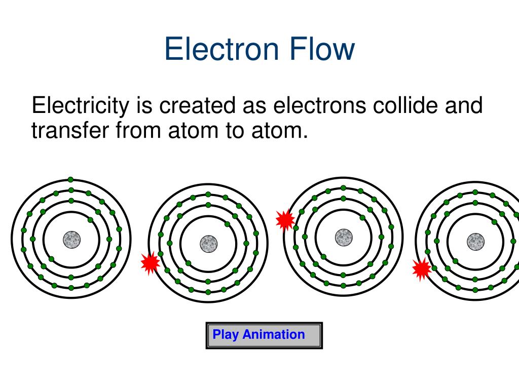
Visualizing Electron Flow in Cutoff vs Saturation Regions
Let me paint you a picture. I’ve spent over a decade staring at oscilloscope traces and probing transistor legs, and I can tell you that the moment the conceptual lightbulb goes off for most engineers is when visualizing electron flow in these two operating modes. It’s not just about memorizing VCE(sat) values or the 0.7V barrier. It’s about seeing the little guys move. Honestly? Half the trouble in circuit design comes from treating a transistor like a magical switch instead of understanding the physics inside the silicon.
We all know a transistor can be a switch or an amplifier. But when it comes to cutoff vs saturation, you are literally looking at two extremes of electron behavior. In one, the party is over, and the electrons have gone home. In the other, they are crammed into the room like a Tokyo subway at rush hour. And if you don’t know how to visualize that traffic jam, your circuits will lie to you. Let’s crack open the hood.
#### The Great Valve Analogy (And Why It Falls Short)
Most textbooks tell you a transistor is like a water valve. Base current opens the gate, and collector current flows. That’s fine for a Friday afternoon explanation. But when we dig into visualizing the electron flow, the valve analogy breaks down hard in cutoff and saturation. Think about it—a water valve either lets water through or it doesn’t. A transistor in saturation still lets current through, but it’s a completely different beast than the linear region. The valve analogy doesn’t explain the voltage drop or the stored charge.
Here’s the real scenario. Imagine a long hallway with two doors at the end. The electrons (your party guests) want to get from the emitter to the collector. The base is the bouncer controlling one of those doors.
- In cutoff, the bouncer is asleep. The first door is completely locked. No guests get in. Zero current. - In saturation, the bouncer is panicking. He opens the first door so wide that guests pile up behind the second door faster than they can leave. There’s a massive traffic jam, but current is still flowing.
That pile-up is the key. It’s the difference between a blocked pipe and a wide-open floodgate that is actually choking its own drain.
##### Cutoff Region: The Empty Highway
When we talk about visualizing electron flow in the cutoff region, the image is almost boring. It’s sterile. The base-emitter junction is reverse-biased or below the knee voltage (0.7V for silicon). There is zero incentive for majority carriers to jump the barrier. Seriously, imagine a desert highway at 3 AM. No cars. No movement. The speed limit signs are still there, but no one is driving. That’s your collector current (IC)—effectively nonexistent except for a tiny, negligible leakage current (ICEO) that you typically ignore unless you’re building a low-power medical device.
Why does this matter? If you are using the transistor as a digital switch, cutoff is the logical “0” or “OFF” state. The voltage at the collector (VCE) sits at the supply rail. It’s high, it’s stable, and there is zero drama. But here is a practical trap I see junior engineers fall into: they assume that because the transistor is “off” (cutoff), the load is fully disconnected. Not always. A small leakage current can light a weak LED or slowly charge a capacitor. When visualizing electron flow here, remember it’s not perfectly zero—it’s just functionally insignificant. Think of it as the door being locked but with a tiny crack under it. A draft gets through, but no people.
##### Saturation Region: The Floodgates and The Traffic Jam
Now we flip the switch. You drive the base hard. Harder than you need to. You are overdriving the base current (IB) to force the transistor into saturation. This is where visualizing electron flow gets fun and non-intuitive. Remember that highway from the cutoff example? Now imagine a stadium letting out after a concert. Everyone is funneling into the same tunnel. They are moving, yes, but they are elbow-to-elbow. That physical crowding is the excess minority carrier charge stored in the base region.
In a normal active region (linear amplification), the collector-base junction is reverse-biased, which helps sweep carriers from base to collector quickly. In saturation, both junctions (base-emitter and base-collector) are forward-biased. This destroys the sweeping effect.
Here’s the critical visual. Electrons flow from emitter into the base. They find the base-collector junction is also wide open (forward biased). So they keep going. But because the collector is biased low (VCE is typically 0.1V to 0.3V), there isn’t enough electric field to pull them out fast enough. The carriers pile up. You get a concentration gradient. This is why saturation is characterized by a low VCE(sat) and a high base current. The transistor is fully ON, but it’s not efficient.
Visualizing the voltage drop is the trick. In cutoff, VCE equals VCC (the supply). In saturation, VCE drops to a small value. This is the transistor acting like a closed switch with a small resistor inside. The lower the VCE(sat), the better the switch. But here’s the kicker: the electron flow in saturation is slower to stop. When you try to turn the transistor OFF from saturation, those piled-up carriers (the traffic jam) have to clear out. This causes storage time—a delay where the transistor remains ON even after you remove the base drive. This is a huge issue in high-speed switching. If you don’t visualize the pile-up, you can’t design around it.
#### Visualizing the Dance of Carriers in Real-Time
Let’s get specific about the carrier movement. Look, in an NPN transistor, the majority carriers in the emitter are electrons. They are negatively charged. In cutoff, the base-emitter junction is reverse biased. The negative voltage on the base repels electrons. They don’t even attempt to cross. The collector sits there, waiting, but nothing happens. It is the equivalent of a dead circuit branch.
In saturation, the base-emitter junction is heavily forward biased. Electrons flood from the emitter into the base. Now, the base is thin and lightly doped. Normally, most electrons would cross to the collector. But because the collector-base junction is also forward biased, the collector is not pulling them. The base becomes saturated with electrons that cannot leave. They literally diffuse around aimlessly until they recombine with holes in the base. This recombination is what creates the base current.
- Cutoff: No injection from emitter. Collector is empty. - Saturation: Heavy injection from emitter. Collector is full (low voltage, high concentration).
One practical way to visualize this on a datasheet is the VCE(sat) vs IC curve. As the collector current increases, VCE(sat) actually increases slightly. Why? Because the traffic jam is getting worse. More cars (electrons) crammed into the same tunnel means more pressure (voltage) is needed to push them through. That’s not a “switch” behavior—that’s a resistive behavior. A perfect switch has zero voltage drop. A saturated transistor has a small one, and it’s a direct window into visualizing the electron traffic.
##### Practical Observations from the Lab Bench
I’ve spent countless hours with a hot soldering iron and a logic analyzer debugging circuits that “should work” but don’t. The number one culprit? Forgetting the storage time effect from deep saturation. You calculate a simple high-side switch. You think 5V on the base is great. But you overdrive it with 10mA of base current when 1mA would suffice. You are now deep in saturation. The circuit switches ON fast, but turning it OFF takes microseconds longer than expected because you have to clear that electron flow pile-up.
Here is a short list of what you can see on an oscilloscope that confirms your mental model is correct:
- Cutoff Region: - Collector voltage sits at VCC (flat line). - Base voltage is 0V or negative (for NPN). - Base current is zero. - Saturation Region: - Collector voltage drops to VCE(sat) (e.g., 0.2V). - Base voltage is higher than collector voltage (for NPN). This is a dead giveaway that the collector-base junction is forward biased. - Base current is high. - Turn-off delay (storage time) appears as a “flat spot” on the collector voltage waveform before it starts rising.
When you see that flat spot on the scope trace, you are literally watching the electron flow clear out. It is a physical phenomenon, not a modeling error. The electrons (or holes for PNP) need time to recombine or be swept away. This is why high-speed switching circuits use Baker clamps or anti-saturation diodes. They prevent the transistor from entering deep saturation, keeping it in the “soft saturation” or active region to minimize storage time. That is a direct application of visualizing electron flow.
#### Common Questions About Visualizing Electron Flow in Cutoff vs Saturation Regions
##### What is the main difference in electron movement between cutoff and saturation?
In cutoff, there is virtually no electron flow from emitter to collector. The base-emitter junction is reverse biased, creating a depletion region that blocks carrier injection. In saturation, the base-emitter and base-collector junctions are both forward biased. Electrons flow heavily from emitter into the base, but they pile up because the collector junction is not reverse biased to sweep them out. This creates a high concentration of excess carriers in the base region.
##### Why is VCE so low in saturation but high in cutoff?
In cutoff, the transistor acts like an open switch. The collector is disconnected from the emitter, so the collector voltage is pulled up to the supply voltage (VCC) by the load resistor. In saturation, the transistor acts like a closed switch with a tiny resistance. The electron flow is unimpeded (though crowded), allowing the collector voltage to drop very close to the emitter voltage (typically 0.1V to 0.3V for silicon). The voltage drop represents the residual resistance of the heavily saturated channel.
##### Does the transistor consume power in the cutoff region?
Yes, but it is negligible. In cutoff, there is extremely high voltage across the transistor (VCE is high) but almost zero electron flow (IC is near zero). Power is the product of voltage and current (P=VI). Since current is essentially zero, the power dissipation is practically zero, only limited by the tiny leakage current. In saturation, the current is high but the voltage drop (VCE) is low, so the power dissipation can be moderate. The worst case for power is usually in the active (linear) region where both voltage and current are significant.
##### How does visualizing electron flow help with circuit design?
It prevents you from making assumptions that kill your switching speed. If you visualize the traffic jam in saturation, you understand why overdriving the base is a trade-off. You get a lower on-resistance, but you get a slower turn-off. It also helps you set the proper base drive. You don’t want to drive a transistor into saturation so deep that it takes forever to turn off, but you need enough drive to ensure it is fully saturated to minimize voltage drop. This visualization directly informs your choice of base resistor value and whether you need a speed-up capacitor or a Schottky clamp.
Shop our range of harting crimp tools. The ergonomic tool body helps reduce workplace injuries and eases operator fatigue keeping costs low and production high. Find a huge range of harting crimp tools at element14 australia. Here you will find a range of these products, if the particular tool you are looking for is not listed. The harting catalog offers a wide range of tools, crimping and many more products for electronic devices. Mouser offers inventory, pricing, & datasheets for harting crimpers / crimping tools. 621205 is a controlled cycle crimp tool designed for machined pin and socket contacts installed in harting rectangular power connector han e series connectors, 16a and 10a. Dmc battery powered tools have been engineered to work with our existing die. View datasheets, pricing and availability from digikey now!
View datasheets, pricing and availability from digikey now! Shop our range of harting crimp tools. Here you will find a range of these products, if the particular tool you are looking for is not listed. 621205 is a controlled cycle crimp tool designed for machined pin and socket contacts installed in harting rectangular power connector han e series connectors, 16a and 10a. Dmc battery powered tools have been engineered to work with our existing die. The ergonomic tool body helps reduce workplace injuries and eases operator fatigue keeping costs low and production high. Find a huge range of harting crimp tools at element14 australia. Mouser offers inventory, pricing, & datasheets for harting crimpers / crimping tools. The harting catalog offers a wide range of tools, crimping and many more products for electronic devices.
Mouser offers inventory, pricing, & datasheets for harting crimpers / crimping tools. Find a huge range of harting crimp tools at element14 australia. The ergonomic tool body helps reduce workplace injuries and eases operator fatigue keeping costs low and production high. View datasheets, pricing and availability from digikey now! Shop our range of harting crimp tools. 621205 is a controlled cycle crimp tool designed for machined pin and socket contacts installed in harting rectangular power connector han e series connectors, 16a and 10a. The harting catalog offers a wide range of tools, crimping and many more products for electronic devices. Dmc battery powered tools have been engineered to work with our existing die. Here you will find a range of these products, if the particular tool you are looking for is not listed.
Here you will find a range of these products, if the particular tool you are looking for is not listed. The harting catalog offers a wide range of tools, crimping and many more products for electronic devices. View datasheets, pricing and availability from digikey now! Find a huge range of harting crimp tools at element14 australia. Mouser offers inventory, pricing, & datasheets for harting crimpers / crimping tools. Shop our range of harting crimp tools. Dmc battery powered tools have been engineered to work with our existing die. The ergonomic tool body helps reduce workplace injuries and eases operator fatigue keeping costs low and production high. 621205 is a controlled cycle crimp tool designed for machined pin and socket contacts installed in harting rectangular power connector han e series connectors, 16a and 10a.