
The History and Future of ASML's EUV Machines
You know that feeling when you open a new toy on Christmas morning, the anticipation, the unwrapping, the sheer joy? I remember the first time I saw a completed ASML EUV lithography machine in a cleanroom. It was not that. It was frustration. It was a decade of promises and failed deadlines. Honestly, it was a miracle it worked at all. To the outside world, these EUV machines are just the gear that makes iPhones faster. To those of us with grease under our fingernails and a decade of machine data in our heads, they represent the single most difficult engineering feat humanity has ever attempted to mass-produce. We are talking about bouncing laser light off microscopic tin droplets to create a beam that can carve features smaller than a virus. It's insane. Let me take you through the messy, brilliant, and deeply weird history of how we got here, and where the hell we are going next.
The 25-Year Overnight Success
Most people think ASML's extreme ultraviolet (EUV) technology just showed up. It didn't. It crawled. For years. I was a junior engineer in 2009 when the first pre-production tool, the NXE:3100, was being demonstrated. Look—that machine was a science experiment. It could expose a wafer, sure, but the power was so low that running it for a full day produced about five usable chips. Five. In the time it takes you to read this paragraph, a modern machine has printed the brain of your smartphone roughly 50,000 times. The gap between the promise and reality was a canyon of shattered dreams. The industry called it "EUVsorrow" for a reason.
The 'Rogue' Plant and the Impossible Dream
The idea started back in the 1980s at Bell Labs and later in Japanese research institutes. Everyone knew that the only way to keep shrinking transistors (Moore's Law, baby) was to ditch the krypton-fluoride lasers and go to a much shorter wavelength. 13.5 nanometers. The problem? That light is absorbed by everything. Air, glass, lenses, dust. Everything. So, the whole machine has to be a giant vacuum chamber. Seriously. You cannot have a single air molecule in the path of that light. To get the light, you hit a 30-micron droplet of molten tin with a 60,000-watt laser twice. The first pulse flattens it into a pancake. The second pulse turns it into a plasma that emits the precious EUV light. It is a controlled thermonuclear explosion happening 50,000 times per second inside a vacuum chamber. It's a big deal.
Why Everyone Almost Gave Up
In the early 2000s, the entire semiconductor industry was screaming for a solution. But the physics was brutal. I remember sitting in a conference in 2006 where a guy from Sandia Labs showed the reflectivity curve of a mirror. A standard mirror reflects 99% of light. For EUV, the best mirror—made of hundreds of alternating layers of molybdenum and silicon—reflects only about 70%. And you need 11 of these mirrors just to get the light from the source to the wafer. Do the math. By the time the light hits the resist, you have lost over 95% of your initial power. It was a nightmare. Many companies, including giants like Nikon and Canon, walked away. They said it was physically impossible to build a production-worthy ASML EUV scanner. They were almost right.
The Physics of Magic Mirrors
Let’s talk about the mirrors. Because without them, you have nothing. These aren't your bathroom mirrors. These are the flattest objects ever created by the human hand. If you scaled the surface of a EUV mirror up to the size of Germany, the biggest bump on it would be less than one millimeter high. That is the level of precision required. We are talking about atomic-level smoothness. The mirrors are coated with the moly-silicon stack I mentioned. But holding that stack is the problem. The mirrors are bolted to a frame, but because the machine itself vibrates from the pumps and the moving stages, the mirrors have to be actively adjusted.
Why Light Hates Air
This brings me to the vacuum, and the contamination. Since EUV light gets absorbed by air, the entire path is in a vacuum. But that vacuum isn't perfect. The tin droplets you use to create the light? They fly out and coat the mirrors. It's like trying to keep your car windshield clean while driving through a paint factory. To solve this, ASML developed a "hydrogen curtain." They flow a thin layer of high-speed hydrogen gas over the mirrors. The hydrogen reacts with the tin to create a chemical that can be pumped away. It is the most elegant, fragile, and terrifying solution I have ever seen. One pump failure and that multi-million-dollar mirror set is ruined.
The Flattest Mirrors on Earth
The people who grind these mirrors are a different breed. They work for Carl Zeiss SMT (a subsidiary that ASML basically owns). They spend months, sometimes over a year, polishing a single piece of Zerodur glass-ceramic. The tool they use? A spinning pad and a specific type of bonnet. It looks like a shop tool you'd buy at a car parts store. The genius is in the process and the metrology. They measure the mirror surface with a laser interferometer, find a bump the size of a single atom, and then rub that bump away with the bonnet. It is brute force meets absolute precision. And they hit the target every time. It's a big deal.
The High-NA Horizon
So, where are we going? The current king is the NXE:3400C and the new NXE:3800E. These are the workhorses, spitting out wafers with a numerical aperture (NA) of 0.33. That is the sweet spot for today's 3nm and 5nm chips. But we are already running out of room. The next step is the massive evolution: High-NA EUV. These new machines, the EXE:5000 series, bump the NA to 0.55. This is not a minor upgrade. It is a completely different optical system.
The $400 Million Gamble
Each High-NA EUV machine costs roughly $400 million. I am not rounding up. The ASML High-NA system is the size of a semi-truck and weighs over 200 tons. It has to be disassembled into 250 crates, flown in a special cargo plane, and reassembled in a cleanroom that had to be built just to hold it. The mirrors are larger, flatter, and there are fewer of them, which is a victory in itself. The biggest change is the anamorphic lens. Instead of projecting a perfect square, it stretches the image by a factor of four in one direction. This allows the larger NA to work without the mirrors getting too big to manufacture. It is a hack. A beautiful, physics-defying hack.
What High-NA Actually Unlocks
For the pure physics nerds: High-NA gives us a resolution of roughly 8nm in the metal pitch. That is the distance between the wires on the chip. This is what will enable the 2nm, 1.4nm, and eventually the sub-1nm process nodes. Without High-NA, we hit a wall. You literally cannot print a smaller transistor with 0.33 NA light. (Unless you use multi-patterning, which is like trying to make a fine sketch by drawing over the same line four times. It works, but it's slow and expensive). The future of High-NA is about power, speed, and yield. ASML has promised 185 wafers per hour on the EXE:5000, which is faster than the current 0.33 machines. If they hit that, the future of computing is secured for another decade.
The Elephant in the Cleanroom
Let's not pretend it's all smooth sailing. I have to be honest with you—the future has serious problems. The biggest issue is the source power. To get the throughput needed for High-NA, you need a EUV source that can deliver over 500 Watts of in-band power. We have this. Barely. But the tin plasma gets more violent at higher powers. You start getting "plasma debris" that erodes the collector mirror (the giant mirror that catches the light from the tin droplet). It's like a sandblaster in your front room.
The Source Power Problem
The industry is chasing 600 Watts and beyond. That is a massive engineering challenge. The lasers themselves need to be more powerful and more stable. The droplet generator (which fires those tiny tin balls at 50kHz) has to be more precise. One tiny sputter and the whole sequence fails. I have seen engineers stand in front of a machine for 18 hours just to get the "drop catch" rate above 99.9%. It is tedious, meticulous work. We are now talking about using "free electron lasers" (FELs) as a source of EUV light for the generation after High-NA. That is an entirely different level of complexity. Think of it like replacing the engine in your car with a particle accelerator.
The Pellicle Nightmare
Another dirty secret is the pellicle. That is the thin membrane, like a film, that sits over the photomask to keep dust off it. In a 193nm (deep UV) machine, it's a simple polymer sheet. In EUV, the pellicle has to survive in a vacuum, be essentially transparent to 13.5nm light (which absorbs in everything), and withstand the heat of the tin plasma. It is a piece of polysilicon only 50 nanometers thick. It breaks. A lot. If the pellicle breaks during a wafer run, you contaminate the entire optical column. Shutting down a fab for a week to replace that pellicle costs millions. The current solution is a carbon nanotube pellicle, but it's still not perfect. Until we solve the pellicle problem for High-NA, every EUV lithography machine is one accident away from a very expensive headache.
Common Questions About the History and Future of ASML's EUV Machines
Why does ASML have a monopoly on EUV machines?
It's not a monopoly from greed. It's a monopoly born from desperation. ASML invested over 20 years and roughly $6 billion in R&D before selling a single production-worthy machine. Their competitors, Nikon and Canon, correctly identified the risk as too high and stayed with older technology. ASML also owns the critical supply chain through investments in Cymer (the light source) and Carl Zeiss (the optics). No other company on earth has the network, the patents, or the insane level of vertical integration to build these things. It is the ultimate barrier to entry.
How long does it take to build one EUV machine?
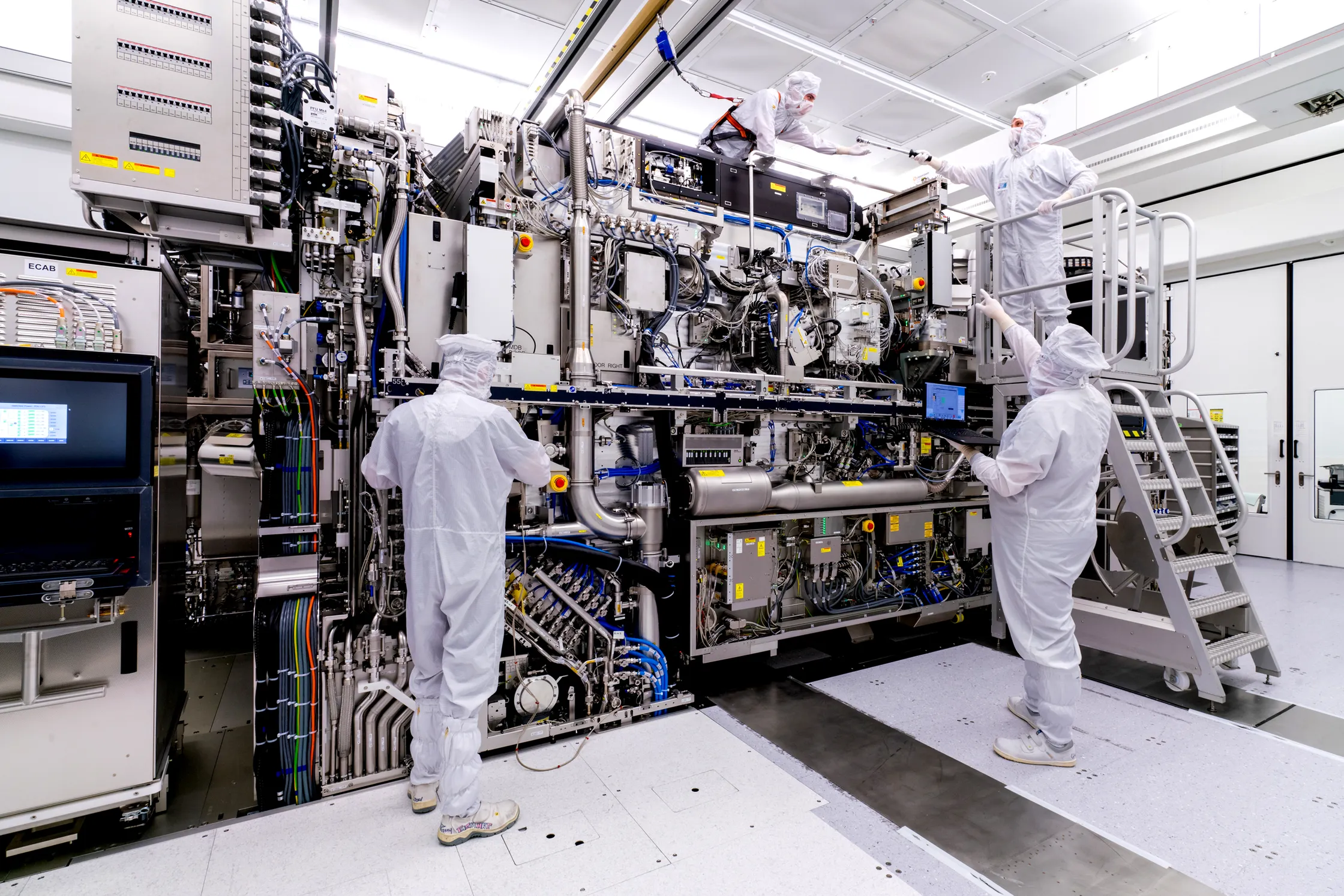
From start to finish, about 12 to 18 months. It takes three weeks just to pump the vacuum chamber down to the required pressure. The entire machine is assembled in a sterile, climate-controlled bay in Veldhoven, Netherlands. Each machine is then "brought to life" over a period of months, running thousands of calibration tests. It's not a factory line; it's a bespoke creation of physics and Swiss-watch-level engineering.
Will High-NA EUV be the last generation of lithography?
Probably not. The semiconductor industry never dies; it just changes. After High-NA (0.55 NA), we will likely need a completely different approach. I am watching "Hyper-NA" or "Multi-Reflective" optics. But the real wildcard is EUV machines that use a completely different source (FELs) or even "direct-write" electron beam lithography. For the next 10 years, High-NA is the king. After that? We are looking at a shift in the physics of light itself. It's a thrilling time to be a skeptic.
Why is the EUV light specifically 13.5 nm?
That wavelength was chosen because of a quirk in physics. Molybdenum and silicon reflect EUV light best at that specific wavelength (due to the constructive interference of their layered structure). Also, that wavelength is technically just inside the "extreme ultraviolet" band, making it easier to work with in a vacuum than shorter wavelengths like X-rays. It was a compromise between reflectivity, source availability, and material science. It wasn't arbitrary; it was the only viable slot in the spectrum.
How does a single machine cost $400 million?
Break it down. You have a 60,000-watt CO2 laser (the size of a small car), a vacuum chamber the size of a room, a set of mirrors that took a year to polish (each costing millions), and a wafer stage that moves with nanometer precision at 5 g-forces. The software to control it all is over 100 million lines of code. The cleanroom floor space alone to install it costs a fortune. It's not a printer. It is a masterpiece of applied physics. You pay for the failure of everyone else who tried to build one.